How to do Should Costing of Semiconductor Packaging?
Disclaimer
This study was conducted entirely in-house by ASI Engineering to demonstrate the capabilities of the xcPEP® platform. The product was independently procured by ASI. No proprietary or confidential information from any other party has been used. Results are not updated after publishing.
Software platforms used for this study
This study is powered by ASI’s proprietary should-costing ecosystem - xcPEP and xcPROC - engineered to deliver real-world accurate, traceable should-costing across mechanical, electrical, and electronics components..
xcPEP delivers real-world accurate, transparent & defensible should cost analysis of mechanical, electrical & electronics components from drawings or physical parts.
Explore xcPEP →xcPROC is the centralized database engine powering xcPEP. Built entirely by ASI’s data research team, each database is meticulously curated to be region-specific and time-specific.
Explore xcPROC →From die singulation to UDFN package
a complete should-costing study of semiconductor packaging.
This blog presents a detailed process study of semiconductor packaging, following every step from die singulation, lead frame preparation, and die attach to bonding, molding, testing, and final tape-and-reel. Through should-costing, we break down how each stage contributes to the overall cost of taking a semiconductor die to a finished IC package.
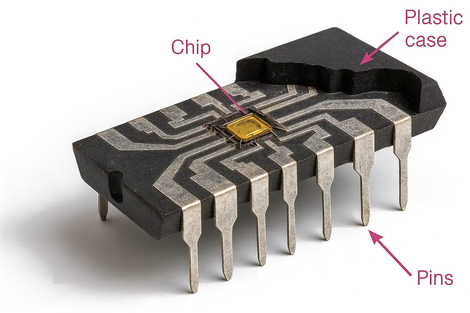
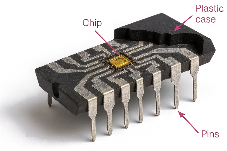
An electronic chip or IC (Integrated circuit) is a compact, self-contained electronic component that performs specific functions such as processing, storage, control, or signal conversion in an electronic system. Semiconductor packaging can account for up to 30% of chip cost, yet sourcing teams often struggle to validate supplier quotes. Rising costs, opaque pricing, and limited transparency in materials, processes, and overheads make cost control challenging. That is why should costing of semiconductor packaging, including UDFN, QFN, and BGA types, is essential for clear cost visibility. Platforms such as xcPEP give cost engineers and procurement leaders fact-based clarity with standardized, transparent costing models—empowering faster, data-driven negotiations.

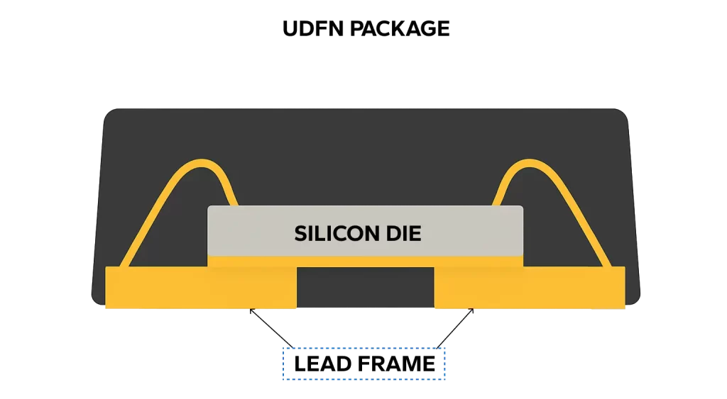
An integrated circuit (IC) contains a silicon die that performs core functions, while the package provides electrical connections, insulation, and protection. ICs come in many package types—such as DIP, UDFN, QFP, BGA, CSP, SOIC, LGA, QFN, PGA, and TSSOP. This blog focuses on the manufacturing process and should-costing of the UDFN (Ultra-thin Dual Flat No-lead) package.
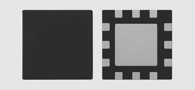
UDFN (Ultra-thin Dual Flat No-lead)
The Ultra Dual Flat No-Lead (UDFN) package is a thin, miniaturized version of the DFN, often under 0.5 mm thick. With a flat, leadless body and metal pads on the underside, it saves board space, reduces profile height, and improves electrical performance by minimizing lead inductance.

UDFN Package Assembly Process
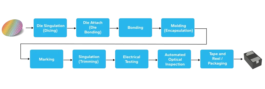
Die Singulation
Die singulation is the process of separating individual dies from a wafer or molded substrate. It defines final die dimensions and prepares each die for packaging, requiring high precision to prevent chipping or damage as devices shrink and wafers thin.
Types of die singulation:
- Blade dicing
- Laser dicing
- Plasma dicing

Cost Drivers:
- Dicing method (saw, laser, plasma)
- Wafer thickness and material hardness
- Street width (saw street size)
- Yield loss due to chipping or cracking
- Equipment speed and precision
Lead Frame Loader
The lead frame loader is an automated system that supplies lead frames—thin metal structures used to support and interconnect the semiconductor die—into the assembly line. It ensures proper orientation, alignment, and continuous feeding of lead frames into subsequent processes such as die attach and wire bonding. Efficient operation of the loader minimizes downtime, reduces handling damage, and maintains consistent throughput in high-volume semiconductor packaging. In should costing of semiconductor packaging, the loader’s automation level, handling precision, and integration with other equipment are critical parameters that directly influence overall cost.
Cost Drivers:
- Loader automation level (manual, semi-automatic, fully automatic)
- Lead frame type (material, thickness, plating)
- Handling precision and alignment requirements
- Equipment speed and throughput capability
- Maintenance frequency and downtime impact
- Integration with upstream/downstream assembly equipment
Die Attach
The semiconductor die is mounted onto the lead frame or substrate using adhesive materials or solder. Die attach is critical for mechanical stability and thermal performance.
Types of die attach processes
- Epoxy die attach
- Solder die attach
- Eutectic die attach
- Silver sintering die attach
- Adhesive film die attach
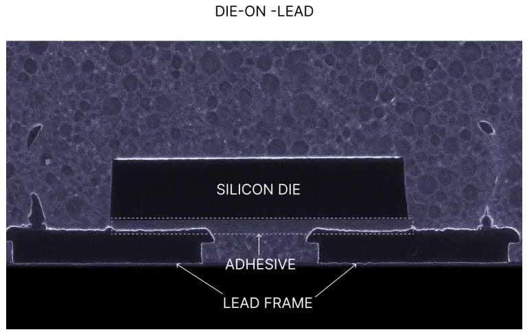
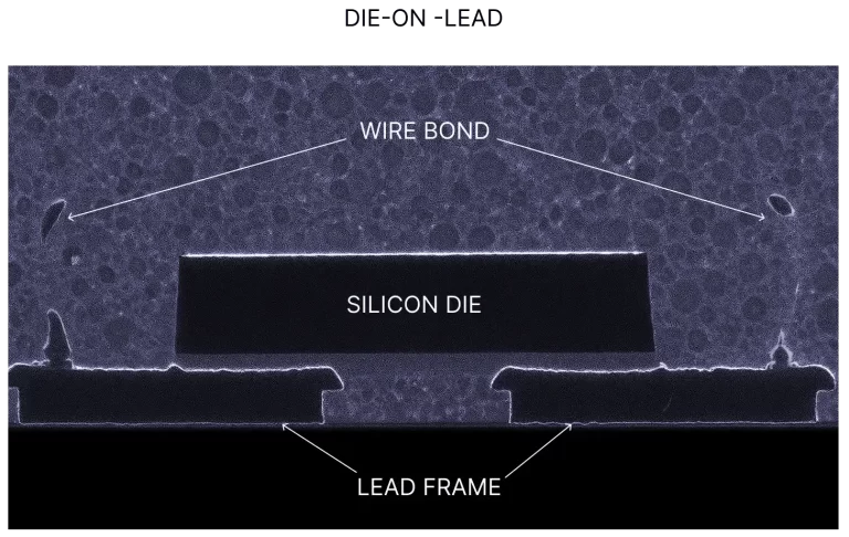
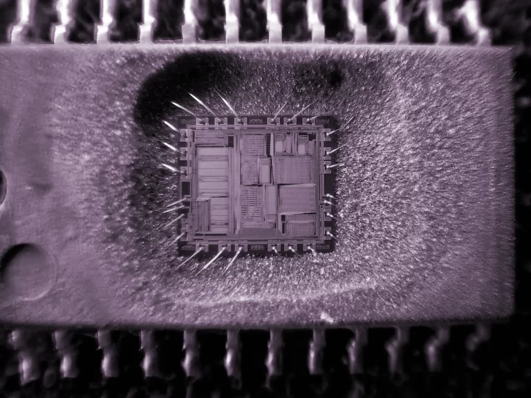
The die attach processes are classified based on the type of adhesive used. The image on the left Below illustrates a silicon die, adhesive layer, and lead frame.
- Adhesive type (epoxy, solder, film)
- Die size and thickness
- Curing or reflow cycle time
- Thermal performance requirements
Bonding
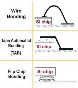
Bonding connects the silicon die to the lead frame or substrate, ensuring chip functionality. The method depends on package type, application, and production volume.
Types of Bonding:
- Wire bonding
- Flip chip bonding
- Tape automated bonding (TAB)
Types of Wire Bonding
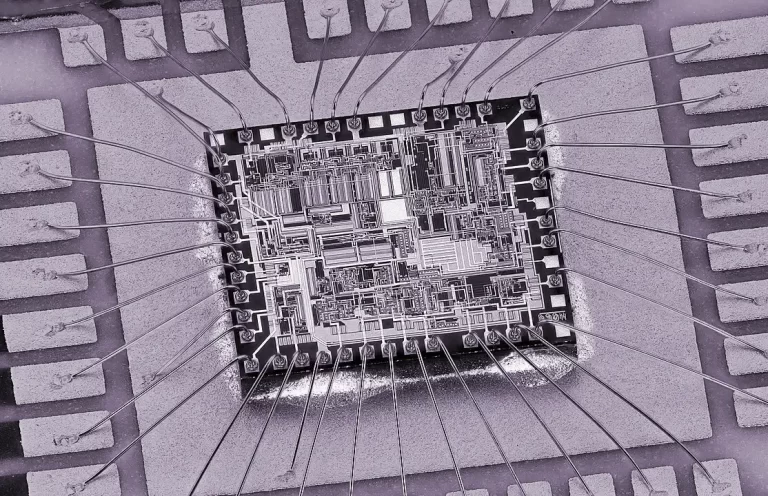
- Ball bonding (preferred in UDFN for speed, reliability, high-volume use; uses Au, Cu, or Al wires 15–75 µm)
- Wedge bonding
- Ribbon bonding
- Heavy wire bonding
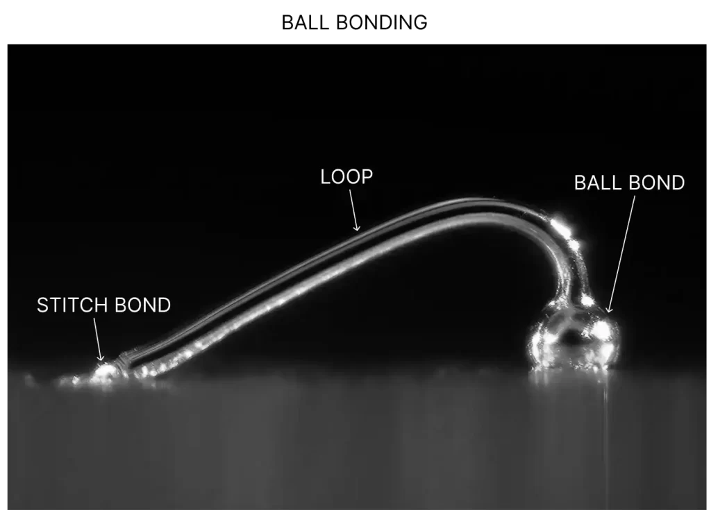
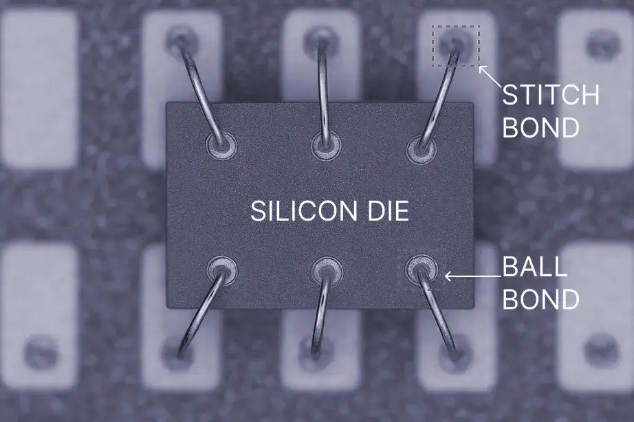
In the above (left) image, ball bond is made at the bond pad of silicon die and stitch bond is made at the bond pad of lead frame as depicted in the image to the right.
Cost Drivers:
- Bonding method (wire bonding vs. flip-chip)
- Wire material (gold, copper, aluminum)
- Bond pad pitch and I/O count
- Equipment speed and precision
- Reliability requirements (thermal cycling, vibration)
Manual Inspection
Manual inspection after bonding is a quality control step where operators visually examine the die bonds and wire bonds using microscopes or magnifiers. The goal is to detect defects such as misaligned wires, lifted bonds, contamination, voids, or mechanical damage. Although slower than automated systems, manual inspection is often used for sampling, low-volume production, or as a secondary check to ensure bonding integrity and yield reliability.
Cost Drivers:
- Labor cost and operator skill level
- Inspection time per unit/package
- Sampling rate vs. 100% inspection requirements
- Yield loss due to defects detected at this stage
Molding (Encapsulation)
Molding uses epoxy-based compounds to encapsulate and protect the die, bonding wires, and internal components from damage, moisture, and contaminants. It ensures insulation, strength, and long-term reliability.
Types of Molding
- Transfer molding
- Compression molding
- Injection molding
- Liquid encapsulation molding (LEM)
- Glop-Top molding
Transfer molding is the most common encapsulation method for UDFN packages. A preheated epoxy molding compound is forced into a mold cavity under pressure, encapsulating the die, wires, and lead frame, then cured with heat to form a durable protective shell.
- Encapsulation method (transfer, compression, liquid)
- Molding compound type and quality
- Package size and cavity design
- Cycle time and curing conditions
- Reliability requirements (moisture resistance, thermal cycling)
Marking
Marking in semiconductor packaging prints identification on the device after molding, ensuring traceability, branding, and compliance.
Methods:
- Ink marking
- Electrolytic marking
- Pad printing
- Laser marking (precise, durable, non-contact; engraves part numbers, logos, date codes)
")

Cost Drivers:
- Marking method (laser, inkjet, pad printing)
- Marking resolution and durability requirements
- Throughput speed of marking equipment
- Customization (logos, 2D barcodes, QR codes)
Singulation
Die Singulation separates individual ICs from an array after assembly and encapsulation, without damaging circuitry.
Methods:
- Sawing (diamond blade, high precision, clean cuts along streets)
- Laser cutting
- Punching

- Singulation method (saw, laser, punch)
- Package size, thickness, and material
- Street width and cutting precision
- Equipment speed and yield loss
- Defect control (chipping, cracking, delamination)
Electrical Testing
Electrical testing is a quality assurance step that verifies a device’s functionality and reliability before shipment. Using automated test equipment (ATE), it measures parameters such as continuity, leakage, threshold voltage, timing, and logic behaviour with high speed and precision.
Cost Drivers:
- Type of test required (functional, parametric, high-speed)
- Test program complexity and duration
- Automated test equipment (ATE) cost and utilization
- Package type and test socket design
- Yield loss due to failed parts
Automated Optical Inspection

Cost Drivers:
- Camera resolution and inspection system type
- Package size, complexity, and surface finish
- Inspection speed and throughput
- Algorithm sophistication (defect detection accuracy)
- False reject rate and reinspection costs
Tape and Reel Packaging
Tape and Reel Packaging is used for automated assembly, where components are placed in carrier tape pockets, sealed with cover tape, and wound onto reels for efficient pick-and-place during PCB manufacturing.
- Tape type and pocket-size precision
- Reel size and material
- Equipment speed and placement accuracy
- Sealing method (heat or pressure)
- Component handling yield (misfeeds, damage)
BILL OF MATERIAL (BOM)
Semiconductor Die
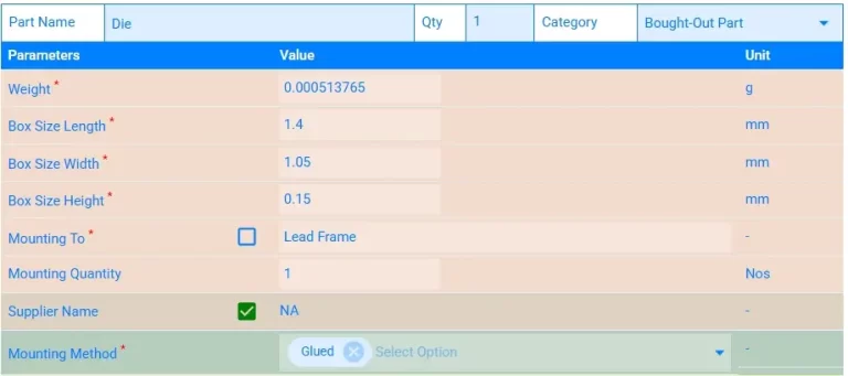
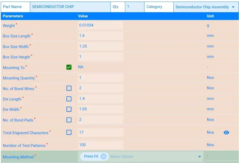
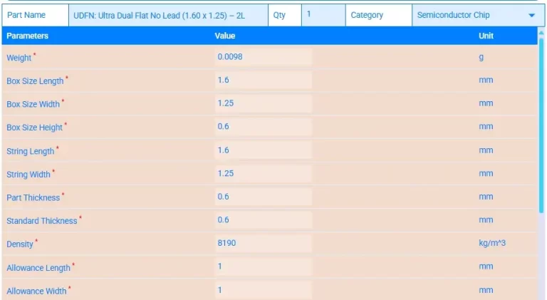
The basic BOM parameters like weight, box size length, width & height in xcPEP are mapped using die weight estimation & image dimension measurement system.
1. Mounting To
The mounting to parameter is lead frame, which means the semiconductor die is attached directly onto the lead frame. This is important because, in UDFN packages, the die is mounted on a copper or alloy lead frame that not only provides the necessary mechanical support but also serves as an electrical path for signal and power connections.
2. Mounting Method
The mounting method is glued. The die is attached to the lead frame using a conductive adhesive. Adhesives such as epoxy or glue are commonly used for small dies, while solder attach is preferred for high-power dies that require better thermal conductivity. The conductive adhesive used is Loctite ablestik 2035SC.
Leadframe
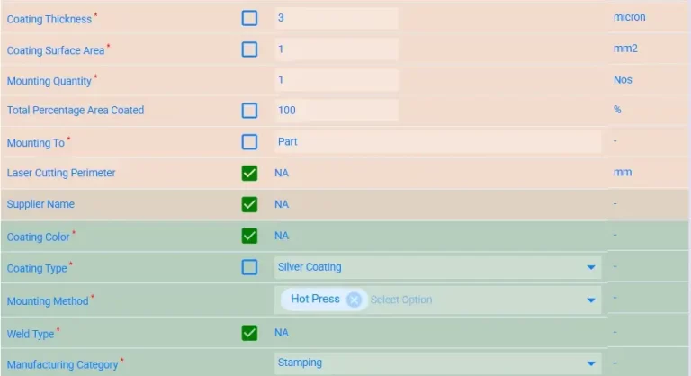
1. Coating Thickness
The coating thickness is 3 microns, meaning a thin layer of silver plating of this thickness is applied to the lead frame surface, which is important because it influences corrosion resistance, solderability, and overall cost.
2. Coating Surface Area
The coating surface area is 1 mm², referring to the portion of the lead frame that is plated, which is full surface coating (100%) and this factor is important because it determines how much plating material is consumed and thus affects cost.
3. Coating Type
The coating type is silver coating, meaning silver is the metal used for plating the lead frame; while silver is commonly chosen for its low resistance and relatively low cost, alternatives such as gold (excellent conductivity but expensive) or NiPdAu (high corrosion resistance) may be used depending on the electrical performance and reliability requirements.
Bonding Wire
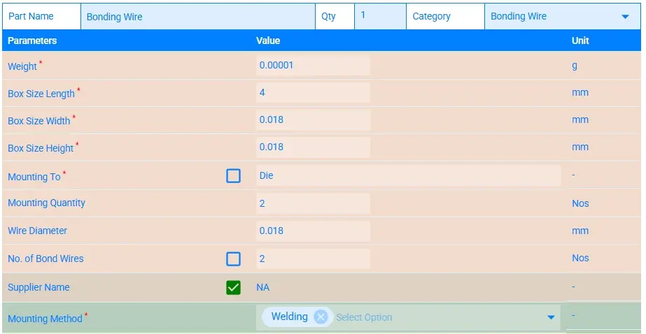
Mounting Method
The mounting method is ultrasonic welding, which means the bonding wire [Cooper bonding wire considered] is attached to the pad using a welding technique, specifically through ultrasonic bonding, where high-frequency vibrations and pressure create a solid metallurgical bond without melting the materials.
Should Costing
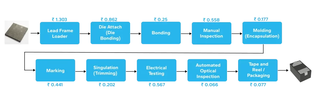
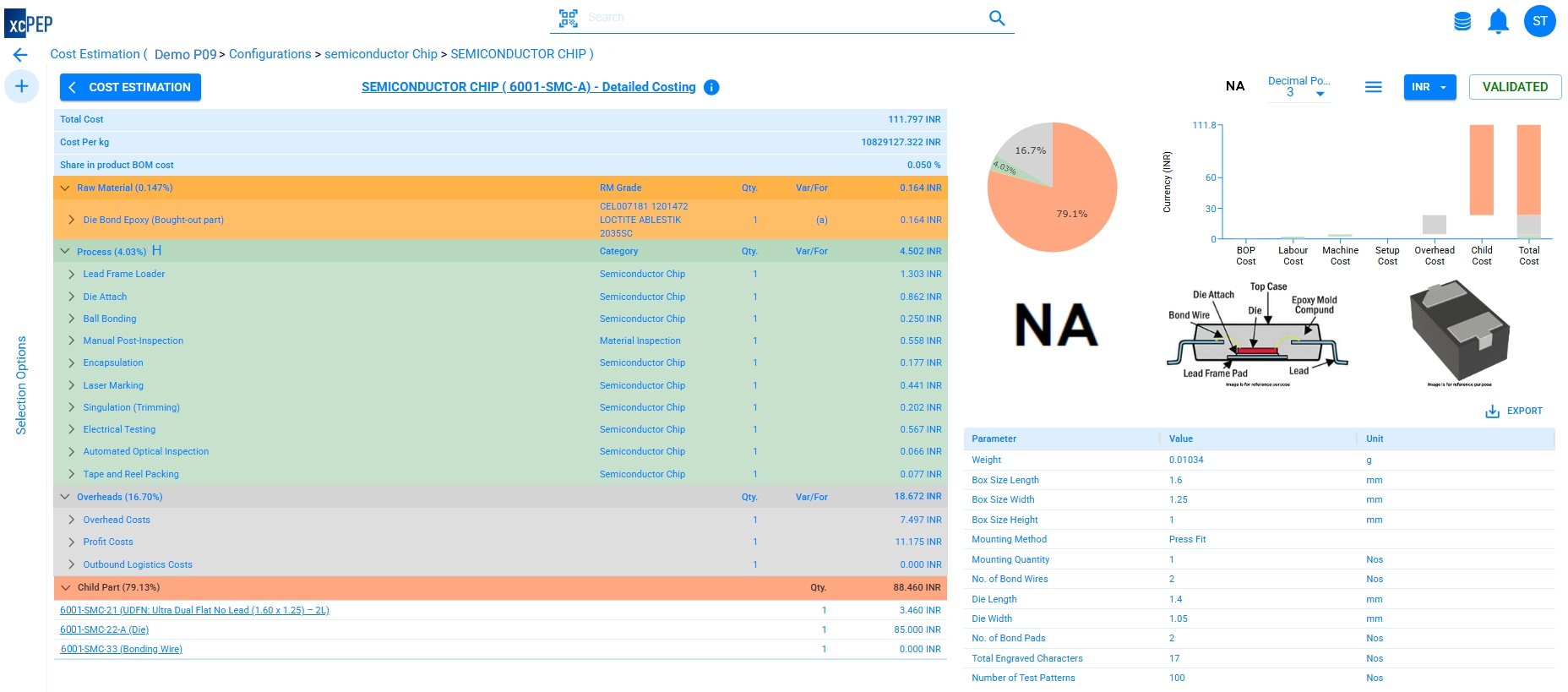
A comprehensive Should Costing (SC) analysis was conducted in xcPEP to evaluate the assembly cost of the IC. The analysis determined that the approximate Assembly cost of the semiconductor was 111.797 INR. Should Costing involves developing assumptions and establishing general guidelines to ensure an accurate and thorough cost evaluation. For the IC assembly, several key assumptions were defined to support the analysis: –
- All final assembly operations for the product are conducted at the manufacturing facility in Bangalore.
- For costing the assembly of “UDFN” package with 2 leads is considered.
- The total planned production output for the year is 500,000 units.
- The costing exercise is based on market data, material prices, and operational rates applicable in February.
- All costing figures are calculated in Indian Rupees (INR) to align with the local manufacturing and procurement environment.
- Costing configuration for semiconductor packaging assembly and lead frame manufacturing are available in xcPEP.
This case demonstrates how should costing of semiconductor packaging provides procurement teams with transparent, data-backed insights into each cost driver, making negotiations and supplier benchmarking more effective
The image below from xcPEP illustrates a detailed cost analysis of semiconductor packaging assembly, breaking down the contributions from raw materials, process steps, and overheads. It provides a clear view of how each component—ranging from packaging materials and assembly processes to labor and facility costs—impacts the overall economics of IC manufacturing
Child Parts
The child parts included in the assembly of semiconductor are as follows: –
- Silicon die
- Lead frame
- Ball bond
- Adhesive epoxy
- Epoxy for encapsulation
Silicon Die
Silicon Die is a small piece cut from a silicon wafer, containing microscopic circuits made through photolithography and deposition. It houses transistors, resistors, capacitors, and interconnects that perform the IC’s logic, memory, signal processing, or power functions.
Lead Frame
1. RM analysis: -
- Base metal type (copper vs. alloy)
- Material grade and purity
- Thickness and width of strips
- Supplier quality and yield
2. Decoiling & straightening: -
- Decoiling:Unwinds coil material into the production line.
- Straightening: Uses rollers to remove curvature and stress, ensuring a flat, uniform strip.
- Coil size and weight
- Straightening equipment precision
- Line speed
- Scrap and handling losses
3. Annealing (Copper): -
- Furnace type (batch vs. continuous)
- Energy consumption
- Temperature and cycle time
- Atmosphere control (inert/reducing gases)
4. Slitting: -
- Strip width tolerance
- Blade/tool wear
- Line speed
- Scrap generated
5. Progressive die stamping: -
Progressive Die Stamping forms lead frames by moving a metal strip through die stations for cutting, punching, and forming until the full pattern is complete.
Chemical Etching (Photoetching): A resist-coated strip is patterned via photolithography, and unprotected areas are chemically etched away to create the lead frame design.
Cost Drivers:
- Die design complexity
- Tool steel type & wear rate
- Press speed and tonnage
- Maintenance downtime
6. Lead frame cleaning: -
Lead Frame Cleaning removes contaminants, burrs, oils, oxides, and particles left after stamping or etching. As lead frames provide both support and electrical interconnects, cleaning ensures reliable die attachment, wire bonding, and plating.
Cost Drivers:
- Cleaning method (wet, plasma, ultrasonic)
- Chemical/solvent cost
- Process cycle time
- Equipment maintenance
7. Microscopic testing - pre coating: -
- Type of microscope (optical vs. SEM)
- Inspection automation level
- Sampling rate
- Operator skill level
8. Silver plating: -
- Plating metal type (Ag, Au, Pd, etc.)
- Thickness of coating
- Electroplating vs. immersion process
- Chemical bath maintenance & yield
9. Coplanarity testing: -
Coplanarity Testing checks that all lead frame leads lie in the same plane. Stamping, plating, trimming, or forming can cause warpage or distortion, and if uncontrolled, leads won’t align properly during die attach, wire bonding, or PCB soldering—reducing reliability.
Cost Drivers:
- Measurement tool precision (laser, optical, mechanical)
- Sampling rate
- Tolerance requirements
- Rework and scrap rate
10. Microscopic tests – post coating
- Resolution and accuracy of inspection tools
- Automated vs. manual inspection
- Sampling frequency
- Defect rework rate
11. Electrical testing
Electrical Testing verifies that packaged ICs meet performance specs after assembly. It ensures the lead frame connections work properly, detecting issues like opens, shorts, or abnormal resistance.
Cost Drivers:
- Test equipment type (parametric, functional)
- Test coverage (all leads vs. sampling)
- Throughput (parallel vs. serial testing)
- False failure/rework rate
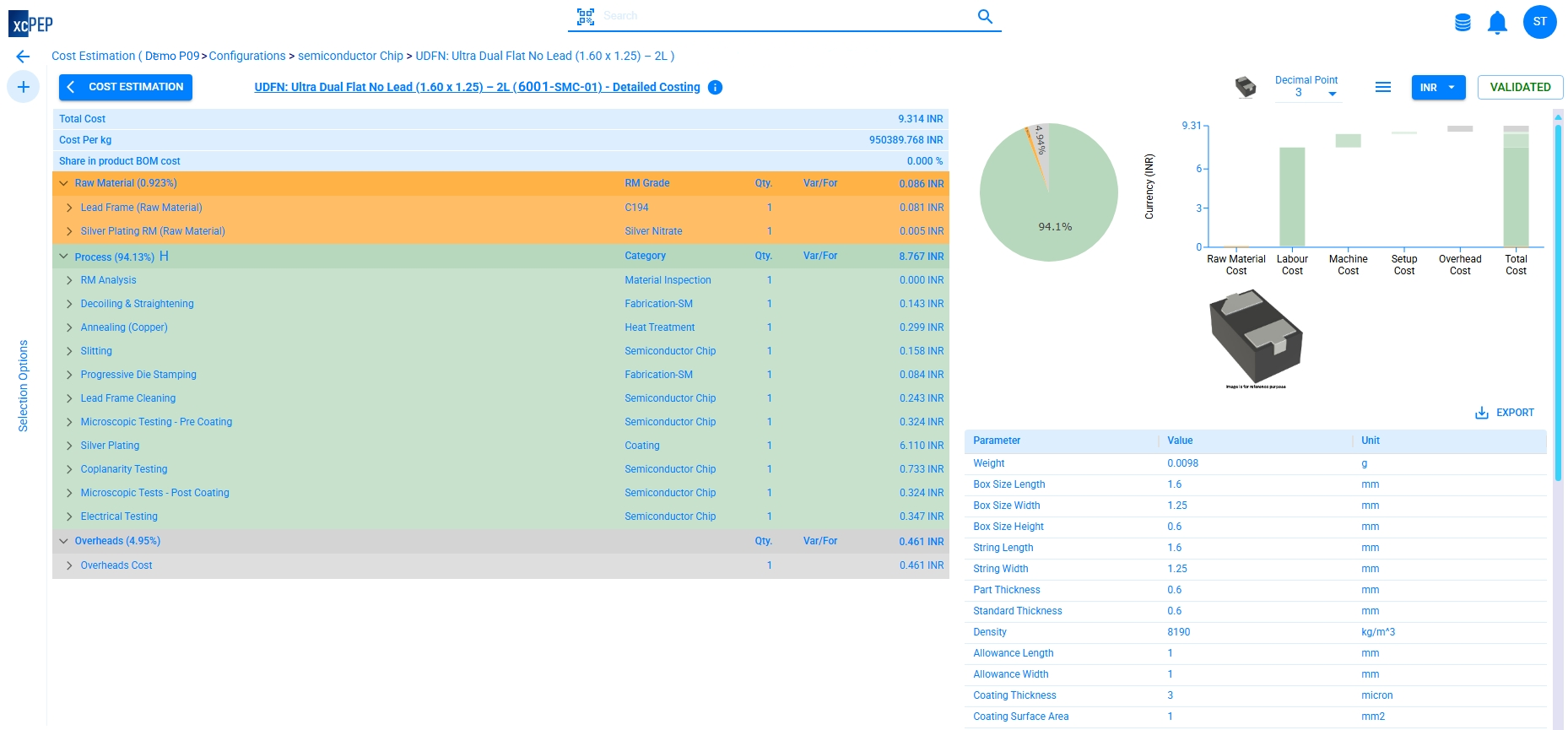
The raw materials used:-
- Copper(C194) sheet
- Silver nitrate
The image below from xcPEP provides a comprehensive breakdown of the cost structure for lead frame manufacturing. It highlights the contribution of raw materials, the various process steps, and the associated overheads, offering a clear view of how each factor influences the overall production cost.
Outcome
The xcPEP analysis highlights that raw materials, overheads, and process-related expenses together define the cost structure of semiconductor assembly. Leveraging this insight allows companies to negotiate faster with suppliers, make fact-based sourcing decisions, benchmark packaging suppliers globally, and identify clear opportunities for cost reduction—turning detailed cost data into actionable strategic advantages.
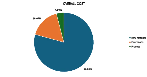
According to the xcPEP analysis it was found that 79.27% (₹88.624) of the total assembly cost comes from raw materials such as the silicon die, lead frame, bonding wire, die adhesive, and encapsulation epoxy. Around 16.7% (₹18.67) of the cost is attributed to overheads, which include indirect expenses like facility rent, utilities, administrative charges, maintenance, and other miscellaneous costs. The remaining 4.03% (₹4.502) is associated with process-related expenses.
This outcome reinforces how should costing of semiconductor packaging enables clear visibility into the contribution of raw materials, processes, and overheads – helping companies pinpoint cost drivers with precision.
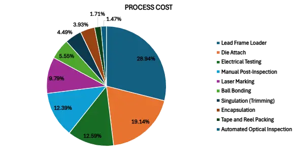
Upon detailed process analysis using xcPEP, the chart below illustrates the distribution of process costs in percentage. Among the various assembly steps, the Lead Frame Loader emerges as the most cost-intensive process, contributing approximately 6.98% and 28.94% of overall process cost of the overall cost. This highlights its significant impact compared to other processes in the IC assembly workflow. By applying should costing of semiconductor processes, each step – from die attach and ball bonding to encapsulation and testing – can be evaluated for its exact cost contribution, giving engineers and procurement teams actionable insights
The silicon die is identified as the most expensive raw material, costing INR 85, which accounts for approximately 76.03% of the total product cost.
This clearly demonstrates how effectively and comprehensively costing can be performed using xcPEP.