PCB Teardown Benchmarking & Cost Reduction Insights
Disclaimer
This study was conducted entirely in-house by ASI Engineering to demonstrate the capabilities of the xcPEP® platform. The product was independently procured by ASI. No proprietary or confidential information from any other party has been used. Results are not updated after publishing.
Software platforms used for this study
This study is powered by ASI’s proprietary should-costing ecosystem - xcPEP and xcPROC - engineered to deliver real-world accurate, traceable should-costing across mechanical, electrical, and electronics components..
xcPEP delivers real-world accurate, transparent & defensible should cost analysis of mechanical, electrical & electronics components from drawings or physical parts.
Explore xcPEP →xcPROC is the centralized database engine powering xcPEP. Built entirely by ASI’s data research team, each database is meticulously curated to be region-specific and time-specific.
Explore xcPROC →At ASI, we employ a variety of activities to ensure accurate and comprehensive benchmarking of PCBs which includes the following:
- Generating the Bill of Materials (BOM) for the PCB
- Mapping the data for electronic child parts
- Creating an architecture diagram for the PCB
- Identifying the layers of the PCB.
- Determining the cost of electronic child parts.
- Calculating the process costs involved in PCB manufacturing
- Generating ideas for PCB cost reduction
- Conducting should costing for the PCB board
- Conducting should costing for the PCB transformer
- Analysing the utilization of the PCB area
In this technical blog, we will discuss deeper into each of these activities and how they contribute to the benchmarking process.
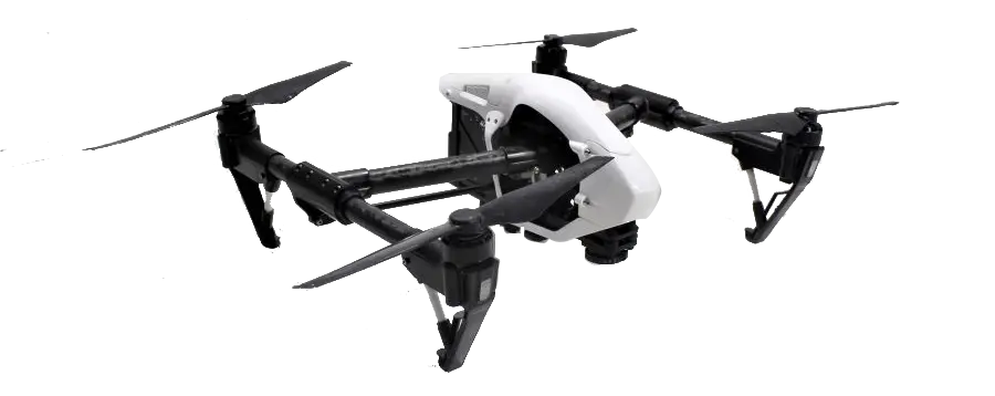
PCB Teardown
Types of PCBs
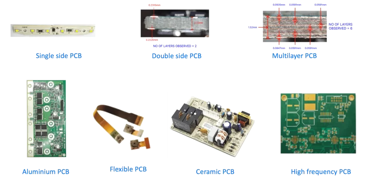
- Single Sided: PCBs with components on one side only.
- Double Sided: PCBs with components on both sides.
- Multi Layered: PCBs with multiple layers of copper and insulating material sandwiched together.
- Aluminium Base: PCBs with a base layer made of Aluminium, used for heat dissipation.
- Flexible: PCBs with a flexible base material, used in applications with tight or irregular spaces.
- Ceramic Base: PCBs with a base material made of ceramic, used for high-temperature applications.
- High Frequency: PCBs designed to operate at high frequencies, with specialized materials and construction techniques to minimize signal loss and interference.
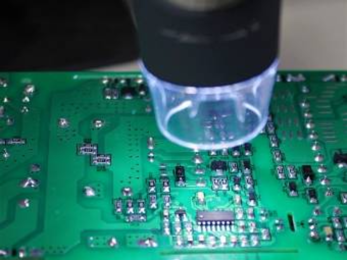
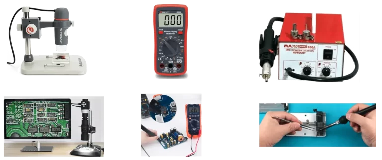
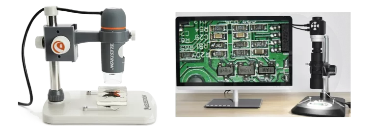
Equipment used for PCB’s study
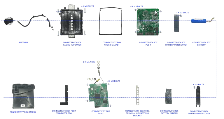
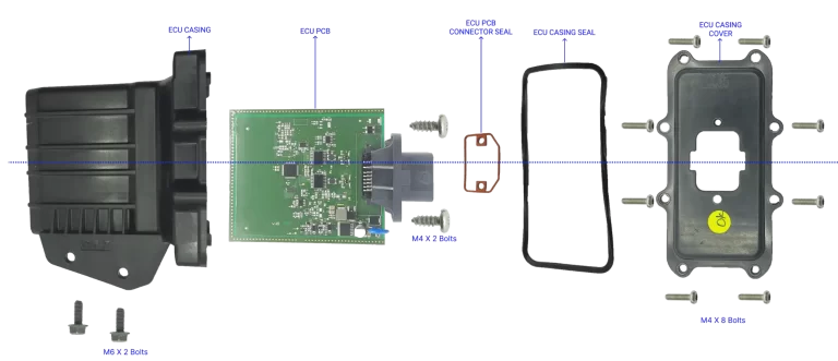
PCB BOM
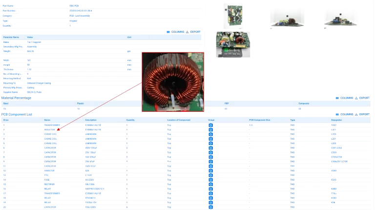
When mapping BOM parameters for a Printed Circuit Board (PCB), it is important to consider several key factors. These parameters include:
- Description: This parameter provides detailed information about the component, including its purpose and specifications.
- Quantity: This parameter indicates the number of components present on the PCB.
- Aluminium Base: PCBs with a base layer made of Aluminium, used for heat dissipation.
- Image: This parameter includes a child part image, allowing for easy identification of the component.
- Location of Component: This parameter defines the side of the PCB where the component is located (top or bottom).
- Type: This parameter identifies whether the component is surface mount (SMD) or through-hole (THD).
- Component Size: This parameter specifies the dimensions of the component, such as the size of resistors or capacitors.
- Component Type: This parameter identifies whether the component is active (such as transistors) or passive (such as resistors and capacitors).
- MFR: This parameter identifies the manufacturer of the child part.
- MPN: This parameter identifies the manufacturer part number or order number of the child part.
- Designator: This parameter identifies the component class according to its name.
- Datasheet: This parameter provides detailed information about the component, including its specifications and performance characteristics.
By mapping these BOM parameters, it is possible to gain a better understanding of the PCB and its components, enabling accurate benchmarking and assessment.
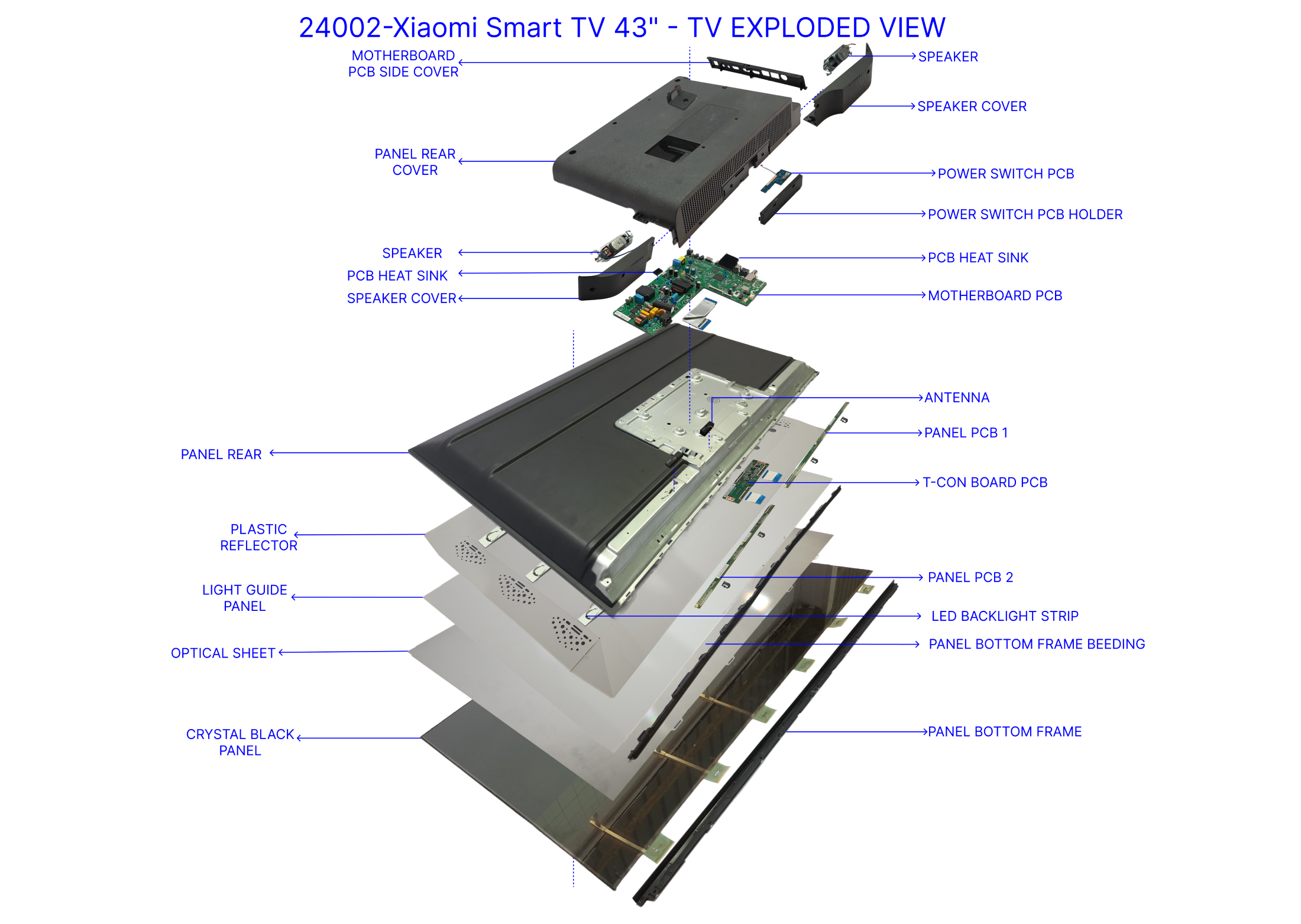
PCB Architecture

PCB layers Identification & Stack up
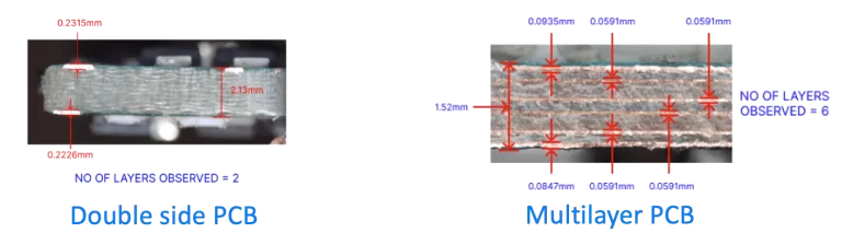
Cross-sectional analysis is a commonly used method for identifying the layers of a PCB. This involves cutting a section of the PCB and examining it under a microscope to identify the copper layers, prepreg, and core thickness. Microscopic images are taken to determine the layer stack-up of the PCB. In addition, copper thickness measurement is often performed using a scanning electron microscope (SEM) to obtain accurate results. By using these techniques, we can gain a better understanding of the PCB’s layer composition and determine any potential issues with the layers or copper thickness.
PCBs can be broadly classified into several types, each with its own specific construction and layer stack-up.
- Single-sided PCBs consist of a single conductive layer and are commonly used in simple circuits where cost is a major concern.
- Double-sided PCBs have two conductive layers separated by an insulating layer and are used in more complex circuits.
- Multi-layer PCBs consist of multiple conductive layers separated by insulating layers and are used in very complex circuits with a high density of components.
- Aluminum base PCBs are used for applications where heat dissipation is a major concern, such as in LED lighting systems.
- Flexible PCBs are made from flexible plastic materials and are commonly used in devices that require bending or shaping.
- Ceramic base PCBs are used in high-temperature and high-power applications due to their excellent thermal conductivity.
- High-frequency PCBs are used in high-speed digital circuits and have a specialized layer stack-up to ensure optimal performance at high frequencies.
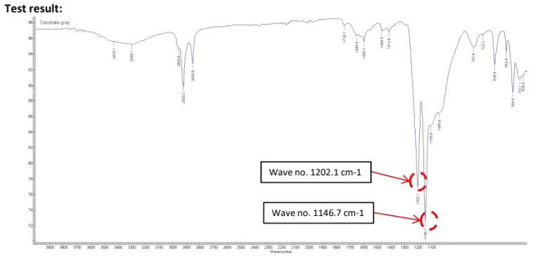
PCB Material Testing


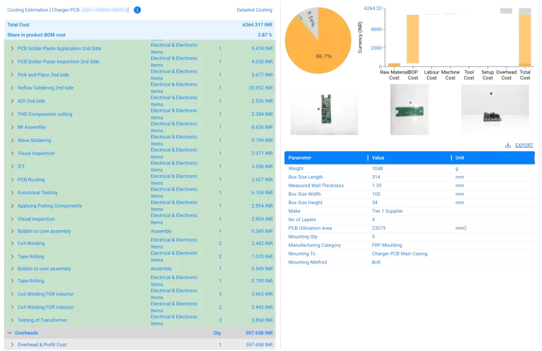
PCB Cost Estimation
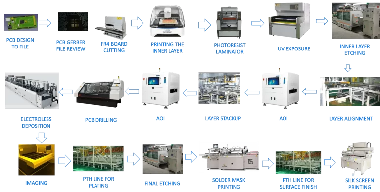
PCB costing is a crucial step in the PCB manufacturing process as it allows the manufacturer to assess the total cost of the PCB, including the cost of raw materials, electronic child parts, and assembly. The cost estimation is done in three stages: Bare Board cost estimation, electronic child parts costing, and Assembly costing.
The first stage, Bare Board cost estimation, involves assessing the cost of raw materials used to manufacture the PCB, including the copper clad laminate, copper foil, and solder mask. The cost is calculated based on the size and thickness of the board, as well as the number of layers.
Surface Finish in PCB:
- Surface finish improves PCB’s flatness, assembly compatibility, electrical performance, and protects against oxidation and corrosion.
- Different surface finishes are available for PCBs, each with advantages in terms of solderability, corrosion resistance, cost, and assembly process compatibility.
- Common surface finishes include HASL, ENIG, Immersion Tin, OSP, Immersion Silver, and Hard Gold.
- HASL is cost-effective and widely used but may not be suitable for fine-pitch components due to an uneven surface.
- ENIG provides excellent solderability and a flat surface but is more expensive.
- Immersion Tin offers good solderability for lead-free processes and a flat surface but is susceptible to oxidation.
- OSP is environmentally friendly, cost-effective, provides good solderability and a flat surface but has lower resistance to handling and environmental factors.
- Immersion Silver provides excellent conductivity and solderability but is more prone to tarnishing.
- Hard Gold offers excellent corrosion resistance and durability but is expensive.
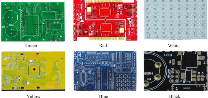
Solder Masks used in PCBs:
- Solder mask is a protective layer applied to PCB surface to insulate and shield copper traces and pads.
- Solder mask is available in various colours such as green, red, blue, black, white, and yellow.
- The choice of solder mask colour is based on personal preference or specific application requirements.
- Green is the most traditional and widely used colour, while red, blue, black, white, and yellow offer aesthetically pleasing and distinctive looks for PCBs.
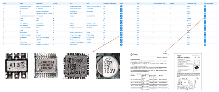
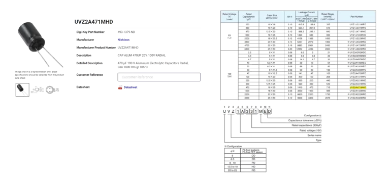
Electronic Child Part Datasheet
PCB Cost reduction Ideas
Idea-1
- Identification and determination of components in the client and competitor’s PCBs.
- Data mapping in xcPEP
- Analysis of the PCB BOM data
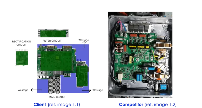
- The client’s PCB consisted of three boards – one mainboard and two smaller secondary boards
- The competitor’s PCB did not have a similar arrangement, and the rectifier and filter circuits were integrated into the main PCB.
- The smaller secondary boards in the client’s PCB were used for rectifier and filter circuits, respectively.
- The competitor’s board utilization was high due to a square layout, while the client’s intricate and complex shape layout resulted in lower PCB utilization.
Idea-2
- Teardown of the PCB from the housing
- PCB BOM mapping under a digital microscope.
- Capturing high-quality images of the PCB and components.
- Connection study and
- schematic mapping
- Schematic analysis
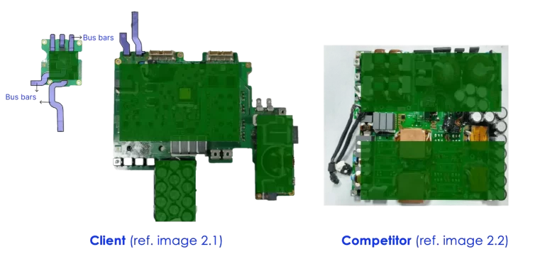
- The architecture study revealed that the client PCB used bus bars for interconnections.
- In contrast, the competitor PCB used regular wired connections for the interface connections of the systems.
- It was proposed to eliminate the busbars and use wired connections, resulting in a cost-saving of 4%.
Idea-3
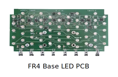
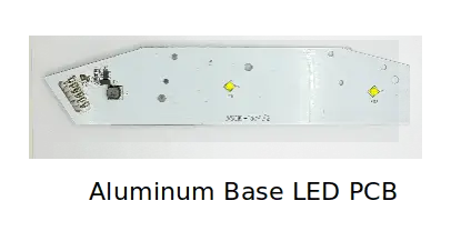
LED lights generate heat during operation and excessive heat can lead to performance degradation or even failure. Aluminum PCBs are preferred over FR4 PCBs for LED applications due to their efficient heat dissipation, lightweight and cost-effectiveness, mechanical stability, and good electrical performance. These characteristics make aluminum PCBs a better choice for LED manufacturers.
It was found that company A was using FR4 base and we recommended them to use aluminum base helping them increase the component’s reliability and reduce cost by 6% at the same time.